Blog Blog
Understanding Electronics Manufacturing and Printed Circuit Board Design
May 18, 2023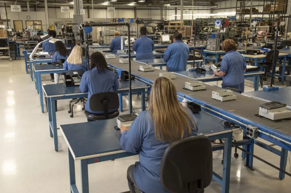
Understanding Electronics Manufacturing and Printed Circuit Board Design
May 18, 2023In today’s rapidly advancing technological landscape, electronics play a crucial role in almost every aspect of our lives. From smartphones and computers to cars and medical devices, electronics have become an integral part of our modern world. At the heart of electronic devices lies the complex process of electronics manufacturing, which involves various stages and components. One key component in the manufacturing process is the Printed Circuit Board (PCB). In this blog post, we will delve into the world of electronics manufacturing and explore the importance and intricacies of PCB design.
What is Electronics Manufacturing?
Electronics manufacturing refers to the process of producing electronic devices on a large scale. It encompasses various stages, including design, prototyping, component procurement, assembly, testing, and packaging. The goal of electronics manufacturing is to transform a concept or design into a fully functional and marketable product. This involves a combination of engineering expertise, manufacturing capabilities, and quality control processes.
Printed Circuit Board Design: The Backbone of Electronics
A Printed Circuit Board (PCB) is a fundamental component of electronic devices. It serves as the skeletal structure that connects and supports various electronic components, such as integrated circuits (ICs), resistors, capacitors, and connectors. PCBs provide a platform for electrical connections, allowing signals to flow between components and enabling the device to function properly.
PCB design involves creating the layout and circuitry that determine the functionality and performance of the electronic device. Designers utilize specialized software to plan and arrange components on the board, ensuring optimal placement for electrical connections, signal integrity, thermal management, and mechanical stability. Factors such as board size, layer count, material selection, and routing techniques are carefully considered during the design phase.
The Design Process
The PCB design process typically starts with capturing the schematic, which is a graphical representation of the circuit’s electrical connections. Designers use Electronic Design Automation (EDA) software to create the schematic, symbolically representing components and their interconnections.
Once the schematic is complete, the next step is to transform it into a physical PCB layout. Designers place components, define the board shape and size, and route electrical connections. They consider factors like signal integrity, power distribution, electromagnetic compatibility, and manufacturability during this phase. Advanced design software provides tools to check for errors, perform design rule checks (DRC), and simulate electrical performance.
The final design files are then sent to the PCB manufacturer, who fabricates the board using specialized manufacturing processes. This involves etching copper layers, drilling holes, adding vias and plating, and applying solder masks and surface finishes.
The Importance of PCB Design
Efficient and well-executed PCB design is critical for the success of electronic devices. Here are a few reasons why:
- Functionality and Performance: Proper PCB design ensures the efficient flow of electrical signals, reducing noise, crosstalk, and other signal integrity issues. It also enables optimal power distribution and thermal management, preventing overheating and maximizing performance.
- Size and Space Optimization: PCB designers strive to create compact and space-efficient layouts, especially in portable devices. Careful component placement, layer stackup, and routing techniques allow for miniaturization and efficient use of available space.
- Manufacturing Efficiency: A well-designed PCB facilitates the manufacturing process. Clear and concise documentation, standardized design practices, and adherence to industry standards enable smooth production, reduce assembly errors, and minimize rework.
- Cost-Effectiveness: Efficient PCB design reduces material wastage and lowers manufacturing costs. Moreover, effective thermal management and proper grounding techniques can prevent component failures, saving on repair and replacement expenses.
Conclusion
Electronics manufacturing and PCB design are essential components of the technology-driven world we live in today. Understanding the intricacies of the electronics manufacturing process and the importance of PCB design enables engineers and designers to create efficient, high-performance, and reliable electronic devices. By continuously pushing the boundaries of innovation in electronics manufacturing and PCB design, we can expect even more advanced and sophisticated electronic devices that enhance our lives in remarkable ways.